Related Questions10 Items
Q1.MCQ
A 3-input majority logic gate has inputs $X, Y$, and $Z$. The output $F$ of the gate is logic '1' if two or more of the inputs are logic '1'. The output $F$ is logic '0' if two or more of the inputs are logic '0'.
Which one of the following options is a Boolean expression of the output $F$?
Q2.MCQ
A full adder and an XOR gate are used to design a digital circuit with inputs $X, Y$, and $Z$, and output $F$, as shown below. The input $Z$ is connected to the carry-in input of the full adder.
If the input $Z$ is set to logic '1', then the circuit functions as with $X$ and $Y$ as inputs.
!image(https://uadmin.udsfgecw.tech/file/download/public/public:7bfffa8b-ca95-491f-80d1-e0a8d09f0476.jpg)
Q3.MCQ
A $10$-bit analog-to-digital converter (ADC) has a sampling frequency of $1$ MHz and a full scale voltage of $3.3$ V.
For an input sinusoidal signal with frequency $500$ kHz, the maximum SNR (in dB, rounded off to two decimal places) and the data rate (in Mbps) at the output of the ADC are \\\\\\\\, respectively.
Q4.MCQ
A positive-edge-triggered sequential circuit is shown below. There are no timing violations in the circuit. Input $P0$ is set to logic ‘0’ and $P1$ is set to logic ‘1’ at all times. The timing diagram of the inputs $SEL$ and $S$ are also shown below.
The sequence of output $Y$ from time $T0$ to $T3$ is .
image needed to be inserted here
Q5.MCQ
!image(https://uadmin.udsfgecw.tech/file/download/public/public:9d30c102-d8e1-4934-9b1a-f8dd93e1c891.png)A positive-edge-triggered sequential circuit is shown below. There are no timing violations in the circuit. Input $P0$ is set to logic '$0$' and $P1$ is set to logic '$1$' at all times. The timing diagram of the inputs $SEL$ and $S$ are also shown below.
The sequence of output $Y$ from time $T0$ to $T3$ is \\\\\\\\.
image needed to be inserted here
Q6.NUMERICAL
A 4-bit weighted-resistor DAC with inputs $b3$, $b2$, $b1$, and $b0$ (MSB to LSB) is designed using an ideal opamp, as shown below. The switches are closed when the corresponding input bits are logic '1' and open otherwise.
When the input $b3b2b1b0$ changes from $1110$ to $1101$, the magnitude of the change in the output voltage $VO$ (in mV, rounded off to the nearest integer) is \\\\\\\.
!image(https://uadmin.udsfgecw.tech/file/download/public/public:71dbe329-adb9-40bf-a44c-48e975688624.jpg)
Q7.NUMERICAL
In a number system of base $r$, the equation $x^2 - 12x + 37 = 0$ has $x = 8$ as one of its solutions. The value of $r$ is .
Q8.MCQ
!image(https://uadmin.udsfgecw.tech/file/download/public/public:c3783554-46ce-4774-8cf7-6c0bbf5554b9.png)The propagation delay of the $2 \times 1$ MUX shown in the circuit is $10$ ns. Consider the propagation delay of the inverter as $0$ ns.
image needed to be inserted here
If $S$ is set to $1$ then the output $Y$ is .
Q9.MCQ
A 4-bit priority encoder has inputs $D3, D2, D1,$ and $D0$ in descending order of priority. The two-bit output $AB$ is generated as $00, 01, 10,$ and $11$ corresponding to inputs $D3, D2, D1,$ and $D0$, respectively. The Boolean expression of the output bit $B$ is .
Q10.MCQ
A full scale sinusoidal signal is applied to a $10$-bit ADC. The fundamental signal component in the ADC output has a normalized power of $1 \text{ W}$, and the total noise and distortion normalized power is $10 \text{ }\mu\text{W}$. The effective number of bits (rounded off to the nearest integer) of the ADC is .
Electronics EngineeringDigital CircuitsMultiple Choice (MCQ)2 Marks
Q8.
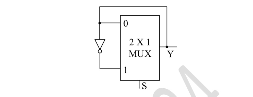 The propagation delay of the 2×1 MUX shown in the circuit is 10 ns. Consider the propagation delay of the inverter as 0 ns.
[image needed to be inserted here]
If S is set to 1 then the output Y is _______.
A
a square wave of frequency 100 MHz
B
a square wave of frequency 50 MHz
C
constant at 0
D
constant at 1