Related Questions10 Items
Q1.MCQ
A 3-input majority logic gate has inputs $X, Y$, and $Z$. The output $F$ of the gate is logic '1' if two or more of the inputs are logic '1'. The output $F$ is logic '0' if two or more of the inputs are logic '0'.
Which one of the following options is a Boolean expression of the output $F$?
Q2.MCQ
A full adder and an XOR gate are used to design a digital circuit with inputs $X, Y$, and $Z$, and output $F$, as shown below. The input $Z$ is connected to the carry-in input of the full adder.
If the input $Z$ is set to logic '1', then the circuit functions as with $X$ and $Y$ as inputs.
!image(https://uadmin.udsfgecw.tech/file/download/public/public:7bfffa8b-ca95-491f-80d1-e0a8d09f0476.jpg)
Q3.MCQ
A $10$-bit analog-to-digital converter (ADC) has a sampling frequency of $1$ MHz and a full scale voltage of $3.3$ V.
For an input sinusoidal signal with frequency $500$ kHz, the maximum SNR (in dB, rounded off to two decimal places) and the data rate (in Mbps) at the output of the ADC are \\\\\\\\, respectively.
Q4.MCQ
A positive-edge-triggered sequential circuit is shown below. There are no timing violations in the circuit. Input $P0$ is set to logic ‘0’ and $P1$ is set to logic ‘1’ at all times. The timing diagram of the inputs $SEL$ and $S$ are also shown below.
The sequence of output $Y$ from time $T0$ to $T3$ is .
image needed to be inserted here
Q5.MCQ
!image(https://uadmin.udsfgecw.tech/file/download/public/public:9d30c102-d8e1-4934-9b1a-f8dd93e1c891.png)A positive-edge-triggered sequential circuit is shown below. There are no timing violations in the circuit. Input $P0$ is set to logic '$0$' and $P1$ is set to logic '$1$' at all times. The timing diagram of the inputs $SEL$ and $S$ are also shown below.
The sequence of output $Y$ from time $T0$ to $T3$ is \\\\\\\\.
image needed to be inserted here
Q6.NUMERICAL
A 4-bit weighted-resistor DAC with inputs $b3$, $b2$, $b1$, and $b0$ (MSB to LSB) is designed using an ideal opamp, as shown below. The switches are closed when the corresponding input bits are logic '1' and open otherwise.
When the input $b3b2b1b0$ changes from $1110$ to $1101$, the magnitude of the change in the output voltage $VO$ (in mV, rounded off to the nearest integer) is \\\\\\\.
!image(https://uadmin.udsfgecw.tech/file/download/public/public:71dbe329-adb9-40bf-a44c-48e975688624.jpg)
Q7.NUMERICAL
In a number system of base $r$, the equation $x^2 - 12x + 37 = 0$ has $x = 8$ as one of its solutions. The value of $r$ is .
Q8.MCQ
!image(https://uadmin.udsfgecw.tech/file/download/public/public:c3783554-46ce-4774-8cf7-6c0bbf5554b9.png)The propagation delay of the $2 \times 1$ MUX shown in the circuit is $10$ ns. Consider the propagation delay of the inverter as $0$ ns.
image needed to be inserted here
If $S$ is set to $1$ then the output $Y$ is .
Q9.MCQ
A 4-bit priority encoder has inputs $D3, D2, D1,$ and $D0$ in descending order of priority. The two-bit output $AB$ is generated as $00, 01, 10,$ and $11$ corresponding to inputs $D3, D2, D1,$ and $D0$, respectively. The Boolean expression of the output bit $B$ is .
Q10.MCQ
A full scale sinusoidal signal is applied to a $10$-bit ADC. The fundamental signal component in the ADC output has a normalized power of $1 \text{ W}$, and the total noise and distortion normalized power is $10 \text{ }\mu\text{W}$. The effective number of bits (rounded off to the nearest integer) of the ADC is .
Electronics EngineeringDigital CircuitsMultiple Choice (MCQ)2 Marks
Q5.
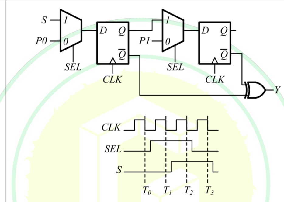 A positive-edge-triggered sequential circuit is shown below. There are no timing violations in the circuit. Input P0 is set to logic '0' and P1 is set to logic '1' at all times. The timing diagram of the inputs SEL and S are also shown below.
The sequence of output Y from time T0 to T3 is ________.
[image needed to be inserted here]
A
1011
B
0100
C
0010
D
1101